On Friday, 8 May 2020 00:25:59 UTC+1, Chris wrote:
On 05/07/20 20:10, Stephen Usher wrote:
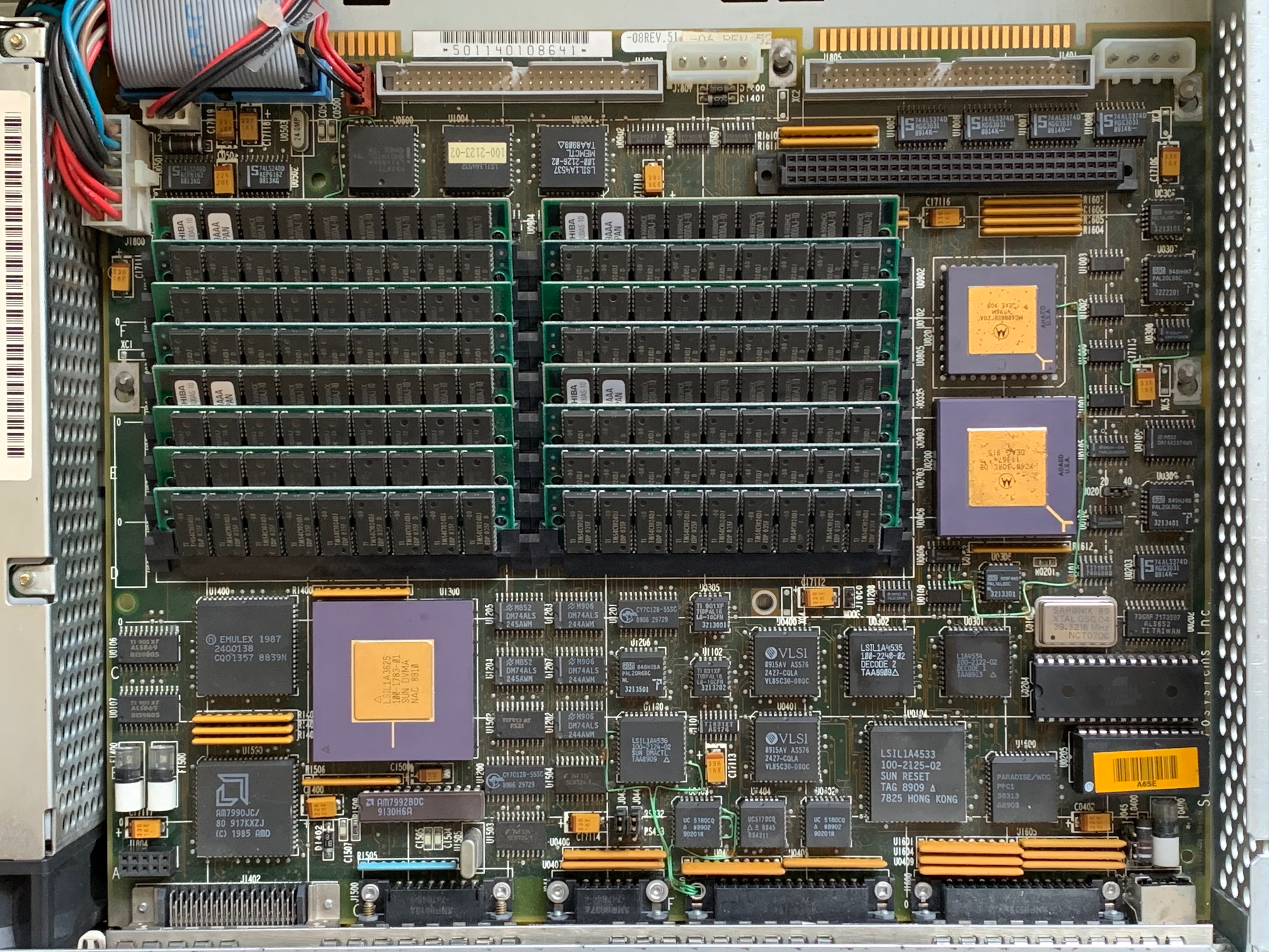
I've a Sun 3/80 with a faulty "decode1" chip and would like to try to reverse engineer it but to do so I need to know the pin-out and how it's connected.
I can get hints of the functionality from the Sun 3/60 schematic on-line but it's different enough to make that information only marginally useful.
Really I could do with a full schematic of the 3/80.
Does anyone know if one still exists and if so how to get it? Or even the pinout of the "decode1" chip would get me a lot of the way given that it's the serial SCC /RD line control which has failed. It *seems* as if the other lines are working so if
I could just replicate that I should be able to get further in the PROM boot/diag process.
Thanks in advance.
If you know what address that rd line is at, you could add a small
daughter board that decodes the address and any control signals
as did the original. Perhaps a small gate array would do the job ?...
Chris
This is the biggest problem, without a schematic I can't work this out properly as the address lines that the chip sees may not be the ones the CPU uses, being generated elsewhere, possibly by the DVMA chip. Also, I'm not actually sure which pins on the
PLCC-44 package *ARE* address lines. There's also a timing issue as the /RD and /WR pulses need to be timed correctly for the SCC to see them properly.
--- SoupGate-Win32 v1.05
* Origin: fsxNet Usenet Gateway (21:1/5)